484-lead Xilinx Spartan6 FPGA PCB Routing
FPGA PCB routing for a 484-lead Xilinx Spartan6 Design
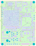
 The picture shows TOP view of a 10-layer (10L) Spartan6 board recently routed at LNAFIN.
The printed circuit board (PCB) has the FPGA chip with 484 BGA-balls, memory in a 144-ball VBGA package, a separate TCP-communication IC, an RJ-45 jack,
etc. plus customer ASIC circuit (144-leads) on the backside.
Economical yet High-performance PCB Routing Solution
The design has one intact ground layer, and two inner ground layers with only a couple of tracks each. Good, solid grounding is a must-have to ensure properly functioning finished circuitry. Three ground layers strucks a perfect balance between cost vs. performance for this design.
Tiny PCB Area Challenge
The PCB area specs was 4.8 x 6.2 cm (1.90×2.45 inch).
Despite the tiny acrage, the most expensive PCB technologies such as buried or blind or laser vias were avoided. All vias were set to use a 0.2mm drill (THT). Minimum track widths and track separations were also kept above 0.1mm (4 mils). With this setup, the design was successfully fit into a total of 10-layers. Thus customer saved a lot of money in PCB fabrication cost. LNAFIN electronics-PCB supplies the low-cost boards to customer together with laser stencil for solder paste application. Assembly service is being discussed with the client.
Picture and all data has been published with customer consent (LNAFIN never publishes project data without customer permission).
