Microwave Circuit Chapter Accessed 8000 Times

Intech Open Access Book on Microwave Circuits

Microwave Circuits Book Chapter on High-speed SiGe and CMOS Buffering
This May 2014 LNAFIN CEO Tiiliharju got this pleasant email from the Intech Open Access publisher:

We are pleased to inform you that your paper “Complementary High-Speed SiGe and CMOS Buffers” has achieved impressive readership results. The chapter you have published with InTech in the book “Advanced Microwave Circuits and Systems” has so far been accessed 8000 times. Congratulations on the significant
impact that your work has achieved to date.

The top downloads of your paper are from the following five countries:
United States of America
India
China
United Kingdom
Germany

The Book Chapter can be found here.

The link gives free access to the chapter. BibTeX reference .bib file can be downloaded here. The chapter discusses different high-speed buffering implementations including CEO’s personal IC implementations in both complementary Sige and nanometer CMOS. Other than our CEO’s chapter, the book has chapters from different microwave circuit experts worldwide. For example the chapter on s-parameter techniques from the Linköping University might be a good reference. The chapter is titled “Mixed-Mode S-Parameters and Conversion Techniques.”

LNAFIN starts its first MMIC project for ESA

Based on our strength in high-speed IC design, we are glad to confirm that LNAFIN Oy has won its first MMIC project contest opened by the European Space Agency. The project includes a Low-Noise Amplifier (LNA) design for the Q-band (30-50 GHz) together with 3D encapsulation for outdoor use. The 3D-package design includes Q-band waveguide (WR22) inputs and outputs. Supporting supply and control logic will be developed in accordance to customer and market requirements. The LNA module will have redundancy with two parallel amplifier units so that best reception can be ensured in all conditions.

The project was actually launched already in November 2013, but due to the tight schedule and other clients’ needs this news post has been a bit delayed. Meantime we have already passed project’s first checkpoint. We will try to add more posts, pictures and results on this LNA-project later. At this point we would like to thank Tekes (the Finnish Funding Agency for Innovation) for their support for this demanding millimeter wave frequency project.

484-lead Xilinx Spartan6 FPGA PCB Routing

FPGA PCB routing for a 484-lead Xilinx Spartan6 Design

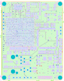
No special vias needed for this tiny BGA-484 PCBThe picture shows TOP view of a 10-layer (10L) Spartan6 board recently routed at LNAFIN.

The printed circuit board (PCB) has the FPGA chip with 484 BGA-balls, memory in a 144-ball VBGA package, a separate TCP-communication IC, an RJ-45 jack,
etc. plus customer ASIC circuit (144-leads) on the backside.


Economical yet High-performance PCB Routing Solution

The design has one intact ground layer, and two inner ground layers with only a couple of tracks each. Good, solid grounding is a must-have to ensure properly functioning finished circuitry. Three ground layers strucks a perfect balance between cost vs. performance for this design.

Tiny PCB Area Challenge

The PCB area specs was 4.8 x 6.2 cm (1.90×2.45 inch).

Despite the tiny acrage, the most expensive PCB technologies such as buried or blind or laser vias were avoided. All vias were set to use a 0.2mm drill (THT). Minimum track widths and track separations were also kept above 0.1mm (4 mils). With this setup, the design was successfully fit into a total of 10-layers. Thus customer saved a lot of money in PCB fabrication cost. LNAFIN electronics-PCB supplies the low-cost boards to customer together with laser stencil for solder paste application. Assembly service is being discussed with the client.

Picture and all data has been published with customer consent (LNAFIN never publishes project data without customer permission).

Prototyping PCB video

Doing prototyping work ? Then watch our video presentation on 4L PCB plus a paste stencil:

Prototyping PCB Do-It-Yourself SMT assembly

Since surface-mount technology (SMT) electronics components are getting more common, electronics enthusiasts need to know their options for prototyping PCB designs which have such elements. Especially the shoestring budget do-it-yourself (DIY) guys have been leveraging painful techniques such as hand-soldering or spreading the solder paste on each pad separately. We wanted to point out that your options also include the use a paste stencil, which can add surprisingly little to the PCB price. A steel solder paste stencil (laser defined or etched openings) lets you squeeze the tin paste onto every component pad simultaneously, which saves a lot of efforts and properly applied also makes the job better. As part of our service we will find the lowest cost solution fitting your component pitch.


Wireless Energy Test Video Published

LNAFIN Wireless Energy Transmission First Test

Wireless energy transmission (WET) has been gaining momentum lately. The Wireless Power Consortium is a standardization organization, which promotes wireless energy transmission techniques.In the last year 2012 this technology finally got some other use than toothbrush charging, when Nokia made it available as a wireless charger for its high-end Lumia 920 model.

Interested in wireless energy transmission ? Then watch our video presentation on youtube:

It is still prudent to say that WET remains a challenge, at least if the devices are not touching and if the power is higher than sub-1-Watt. In this video we take a little step towards that difficutl region. Our results include transmission distances in excess of 2.5 cm and powers around 1 Watt. Also some tweaking to the energy transmission path is suggested at the end of the video.

Notes on LNAFIN & Circuit Boards to Start 2013

PCB and Other Issues to Start a New Year with!

Our printed circuit board and electronics products found their first customers in Finland in 2012, so the end of the year 2012 did not see many blog postings from us! This is gonna change, especially as these English pages have now been published.

Good PCB Customer Response to Start 2013

It is a great pleasure to report that we have happy customers. A direct quote (with customer permission) explains it best:

  • Today i get from Post office my PCB boards. They look absolute great!!
    There was no need of that text layer on top, but otherwise .. look
    fantastic, and already i wish to start soldering elements :-)
    Thanks again and for sure my future orders will be from your company !

Laser-cut steel paste stencils from LNAFIN with the best possible price-quality ratio!We have also delivered Laser paste stencils in 2012!

A framed paste stencil much like the one shown here has been delivered to our customer to start 2013. Pre-tensioned in a steel frame, the 0.12-mm steel paste stencil performs well when it is used in administering ROHS tin paste to dense PCB layouts (the picture is shown with customer permission).


WWW-pages for LNAFIN Electronics and PCB Products

To increase awareness of our electronics and printed circuit board products in Finland, we decided to set up a Finnish version of our web-pages. At the same time the idea was born to start a blog. This is the result of those thoughts, and we call it the Tekno! blog. At the same time, this replaces our Facebook and Google pages as the company news media. These social site pages plus our Twitter account will be refreshed via wordpress plugins.


Paypal Accepted

LNAFIN accepts Paypal (Visa, Mastercard).We now accept Paypal! Paypal is the world’s biggest internet payment method. Customers can now pay for LNAFIN products with their credit cards (Visa, Mastecard) or by using their account at Paypal. Additional information on our payment methods can be viewed here.


1 2 3