LNAFIN Oy Blog pages

LNAFIN Oy Blog pages
LNAFIN Oy Blog posts about designs and RF-MMIC test tools.
Post Categories:

LNAFIN Oy Blog pages have news, development notices and videos about our products and services such as PCB Layout Design, RF-MMIC design and advanced PCB products and services. You can read the posts directly below, or access them via the categories listed above. The Q-band LNA category includes posts about our Q-band LNA MMIC design project for the European Space Agency (ESA), whereas Technical category includes LNAFIN Oy PCB layout and other design articles, our patent information etc.
Published design data is either from our own R&D projects, or it has been included with customer permission.

LNAFIN2 is a Q-band LNA

MMIC Design Sheet: LNAFIN2 is a Q-band LNA

Esa Tiiliharju, doct.tech(EE), LNAFIN Oy, https://www.LNAFIN.com/, eti@LNAFIN.com

MMIC Information

This web-page is re-production of a MMIC design sheet we have assembled for our Q-band LNA project. This chip has been recently fabricated and its simulated performance is shown in this post. The chip fabrication is part of our Q-band ESA project blogged here. The low-noise amplifier has 4-stages, and it has a simulated state-of-the-art performance with low Noise Figure (NF), high gain and good broadband 50-Ω matching.

  • Circuit Name: LNAFIN2, Circuit Function: Q-Band Low-Noise Amplifier (LNA).
  • MMIC size: 3×2 mm2.
  • Foundry: Ommic 70-nm mHemt D007IH.

One stage stability analysis with the probe-method.

Stability verification example using the gprobe2-method. Circuit response is stable in all
loading conditions when probed values remain within -1. . . +1.

Simulated Performance Table

Parameter Unit LNA#2
Centre frequency GHz 40.0
Bandwidth GHz 12.8
Gain dB 31.4
Noise figure dB 1.2
Output 1-dB compression dBm 4
Input return loss dB 22.4
Output return loss dB 21.9
Stability   Unconditional
DC power consumption mW 153.6
Operating temperature °C -25 to +75
PORT1 bw RL=18 dB GHz 14.8
PORT2 bw RL=20 dB GHz 66.1

Note: linearity (1-dB compression) is limited by the small-signal models, which have
only few biasing points. We have done the large signal simulations with biasing points, which correspond to tabulated small-signal characteristics.

Simulated 2-port Characteristics

S21 and S11 of the Q-band LNA.

Simulated 2-port Characteristics: LNA_MMIC_2port 1

Simulated NF performance of the Q-band LNA.

Linear stability factors of the Q-band LNA.

LNAFIN Oy at Alihankinta 2016

Alihankinta 2016 Logo


LNAFIN Oy Participates in Alihankinta 2016 Trade Fair

Alihankinta 2016 is the foremost international industry trade fair in Finland. Industrial subcontractors have been gathering to Tampere for years to gain visibility, new business contacts and new ideas. The Alihankinta fair is held annually in Tampere Exhibition and Sports Centre, Ilmailunkatu 20, 33900 Tampere, Finland. This year’s fair has attracted 1000 exhibitors from 20 countries. As a result of that, the exhibited products and services vary tremendously. However, Alihankinta Fair main product categories have been categorized as: production methods, products and components, R&D and design services plus ICT. Thus we feel that LNAFIN Oy PCB layout design, PCB deliveries, electronics assembly, R&D services, wirebonding, prototyping and RF design know-how has something to offer for Alihankinta 2016 visitors.
LNAFIN-C-hall_300x317

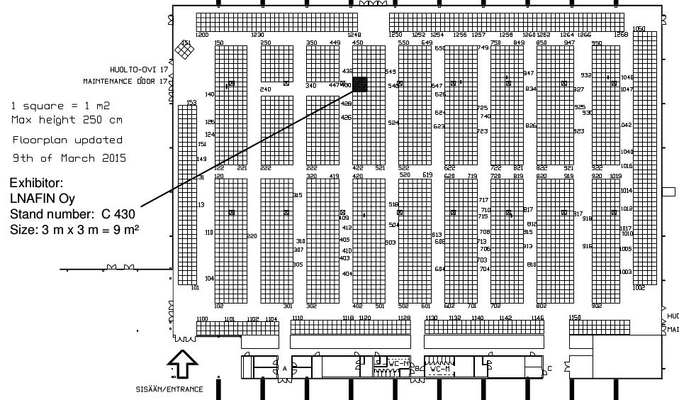
Visit LNAFIN at C430 and Win!

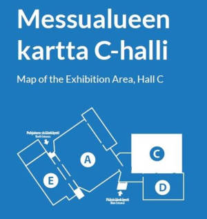
You will meet us in C-hall at our booth C430. We are very satisfied to have gotten a booth in this year’s outsold event. At the same time we wish that many fair goers would have an interest in electronics products and design services. We would be pleased to discuss circuit design and printed circuit board related prototyping/production needs. All booth visitors can take part in our small fair lottery. We will randomly draw winners to receive gift certificates for our products. Winners will be personally informed. We have included two maps of the area in this post: the blue map above shows the general exhibition area layout, whereas the black-and-white map below shows the C-hall exhibitor map.LNAFIN Oy Alihankinta 2016 C430 map
LNAFIN Oy Trademark (TM) Registered

LNAFIN Oy registered TrademarkLNAFIN Oy Trademark Registration Celebrates Exports to 6 Countries Worldwide

To celebrate our starting sixth year in business, we have registered our trademark (TM) at the Finnish Patents and Trademark office. Our trademark LNAFIN cube logo is shown here with the famous circled R-letter. Its basic idea is to combine words LNA and FIN in a graphic form. LNA stands for Low-Noise Amplifier, which is a key block in most radio systems. We have one US patent on LNA structures. As for FIN: that stands for Finland. LNAFIN Oy operates from Helsinki, Finland, and we also wanted to give credit to great Finnish RF and electronics engineers.

Growing customer base has been one of the key reasons for TM regisration. This Spring our export destination count reached 6 different countries such as: USA, Russia, Denmark, Great Britain etc. We appreciate our customers’ trust very much and we will live up to it in the future too. We have delivered various printed circuit board related products such as PCB design, PCB sales and electronics assembly services.

Sprint Layout files for PCB production!

LNAFIN Oy now Adds Sprint 6.0 Files for accepted PCB Production Data

Sprint Layout acceptedSprint PCB layout design program is useful for the printed circuit designer who wants to layout designs directly without schematic entry or any such complexities. This simple productive tool offers professional PCB layout capabilities such as design reuse etc. and is thus very popular both in professional and hobbyist circles. In recognition of that, LNAFIN Oy has decided to start accepting native sprint files for PCB deliveries. These can also be used for prototype and series PCB assembly services when good Bill-of-Materials (BOM) is also included in the zip-file.

Several PCB Layout Programs Supported

LNAFIN Oy has long supported several PCB layout programs such as: Mentorgraphics PADS, Eagle, and KiCAD. PCB layout design services are also available using these tools as based on customer schematic files. The Sprint data format complements our previously supported express-PCB PCB production in the sense that both tools focus on layout-only PCB approach. Here’s the Sprint quick logo for those who recognize that better:
Sprint Layout accepted

LNAFIN Oy Features in an MMIC LNA Design Article in 2014

Waveguide Packaged MMIC LNA Design Draws Attention

LNAFIN Oy got featured in an NI (formerly AWR Corporation) design article in October 2014. The article is titled “LNAFIN Designs MMIC LNA Module for 40 GHz Space
Application Using NI AWR Design Environment.” The article features MMIC LNA design results, which were achieved recently so as to meet a very demanding Q-band LNA specification. Since the LNA is waveguide (WG) packaged, the design tasks include: design and optimization of the WG-to-PCB transitions, supporting PCB design and the MMIC design challenge itself. For example bonding wire compensation as part of the matching network has to be accomplished at the same time as a successful waveguide design is realized.
MMIC LNA waveguide input
One designed WG-to-PCB transition has been shown in the attached figure. The figure includes 3D mesh which is utilized by the EM-simulator used (MWO Analyst). Low insertion loss results around 0.2 dB were obtained, which helps to achieve the specified NF-values towards 1 dB @40GHz. Yet at the same time gain should exceed 25 dB and the matched input and output bandwidths should be wide (>5 GHz).

The full article can be downloaded from the NI website at:
https://www.awrcorp.com/customer-stories/LNAFIN.


New Address

We have relocated to bigger office space in Helsinki Hermanni area. The place is conveniently located as it lies at a 3 km distance from both the Helsinki Main and the Pasila Railway stations. Moreover, the drive  to the Helsinki-Vantaa International Airport takes only 19 minutes.
New address: Orioninkatu 4, 00550 Helsinki, Finland.
Please note that the PO.Box 28 address we previously had for mail has been closed!
All mail should be send to our office in Orioninkatu.

1 2 3